| Welcome to the Plasmonics and Nanosensing Lab!
The Plasmonics and Nanosensing Laboratory is associated with the Graduate School of Pure and Applied Sciences at the University of Tsukuba.
At the Plasmonics and Nanosensing Laboratory
we conduct research directed at developing new types of sensors with nanometer
dimensions that exploit nanoscale physical, electronic, optical and chemical
effects. We are also working to engineer the surfaces and interfaces of
nanoscale sensors in order to optimize sensor performance as well as to study
fundamental processes related to molecular adsorption and binding.
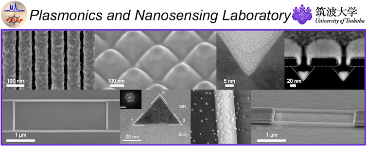
We use, and invent, microfabrication and nanofabrication techniques to realize functional nanoscale devices, and apply this expertise to design, fabricate, and characterize novel electronic, optical and mechanical devices and sensors. We have basic knowledge in surface chemistry and extensive experience in packaging and integration of sensors into microfluidic platforms and the associated design and implementation of microfluidic hydraulic systems for the preparation of nanoliter volume samples. We have expertise with many different characterization and measurement techniques including sub-nanoampere electrical current measurements, atomic force microscopy, optical interferometry, laser confocal optical microscopy and spectroscopy, laser confocal Raman spectroscopy, dark-field optical scattering spectroscopy and conventional optical microscopy.
Contact: Dr. Edwin T. Carlen
|

